
From scientific evidence toward open silicon.
Connect literature, patents, materials, lithography, metrology, experiments, device physics, circuits, RTL, verification, and public-PDK implementation in one traceable workspace.
Evidence intake
Experiment planning
RTL architecture and verification
Example study
From “tiny AI engine” to a real synthesized hierarchy.
This study is understandable at a glance—numbers flow through a grid—but it exercises the disciplines that make open chip design real: interfaces, signed arithmetic, accumulation width, reset, timing of data movement, lint, synthesis, provenance, and honest implementation boundaries.
16
Parallel processing elements
A retained 4 × 4 systolic hierarchy
16 MAC/cycle
Peak architectural parallelism
After the wavefront fills the array
64 / 64
Reference outputs matched
Independent cycle model versus integer reference
12,961
Generic Yosys cells
937 sequential and 12,024 combinational
01
Design briefStart with a recognizable chip idea
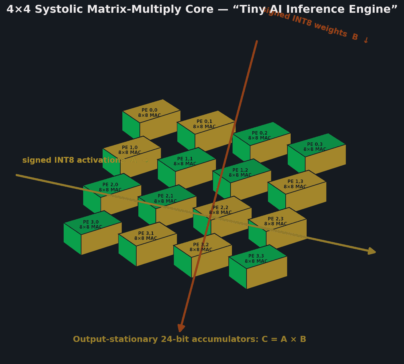
The brief is a tiny AI inference engine: multiply two signed 4 × 4 integer matrices while many small processing elements work in parallel.
02
ArchitectureDesign the data movement
Signed INT8 activations move horizontally, signed INT8 weights move vertically, and each processing element accumulates into a 24-bit result.
03
Numerical modelMake the wavefront visible
A cycle model shows 64 multiply–accumulate operations sweeping diagonally across the array and checks four matrices against an integer reference.
04
Targeted correctionLet the guardrail find a real defect
The first managed lint stopped on two redundant unsigned comparisons. Vicena preserved the failure, removed only those comparisons, and kept the architecture unchanged.
05
Managed computeSynthesize the corrected RTL
Verilator 5.032 passed lint, Yosys 0.52 reported zero check problems, and the managed netlist retained all 16 named processing-element instances.
06
Design evidenceInspect what was actually built
The hierarchy, netlist, generic logic-cell composition, checksums, scorecard, and exact job provenance remain available for review and the next implementation stage.
Real workflow artifacts
Architecture, behavior, and netlist tell the same story.
The notebook begins with the human model of the chip, makes the parallel wavefront visible, checks the arithmetic reference, and finishes with figures parsed from the managed Yosys netlist.
A tiny AI engine made of 16 cooperating processors
Activations and weights enter along different axes. Every processing element performs signed 8 × 8 multiply–accumulate work and retains a 24-bit result.
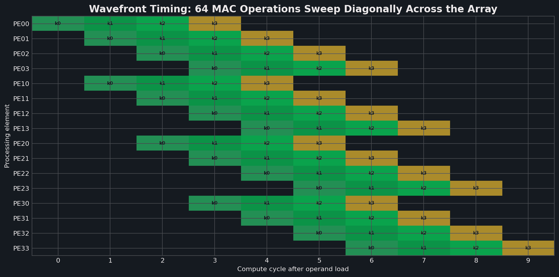
The computation moves like a wave
The timing map makes concurrency concrete: four inner products traverse each row and column while the active diagonal advances across the array.
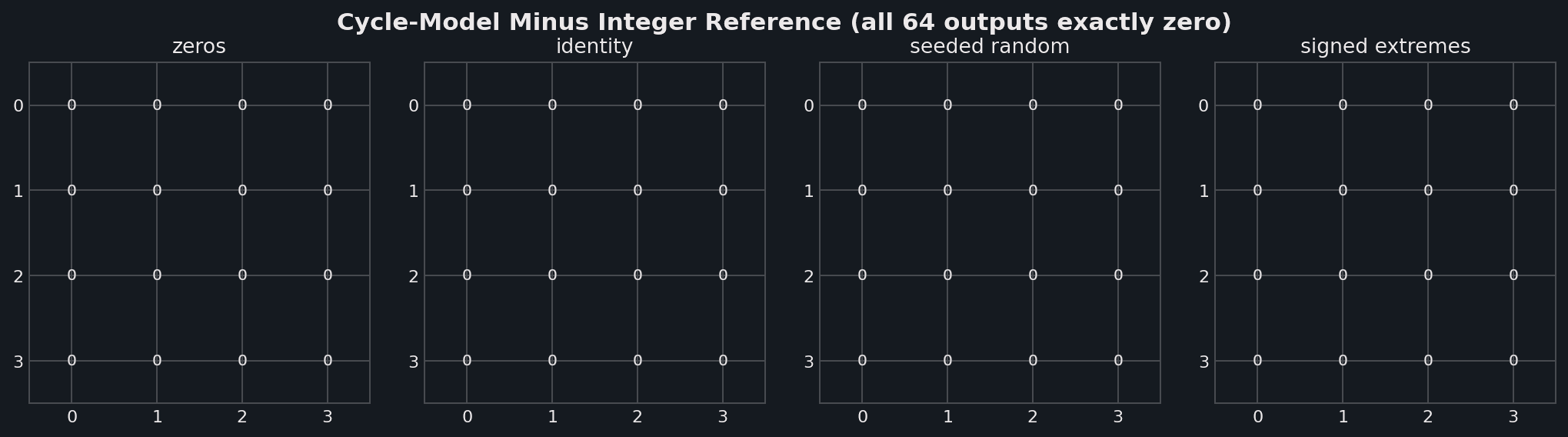
Every cycle-model result matched
Four matrix cases—including signed extremes—produced 64 exact matches against the integer reference. This is cycle-model evidence, not RTL simulation.
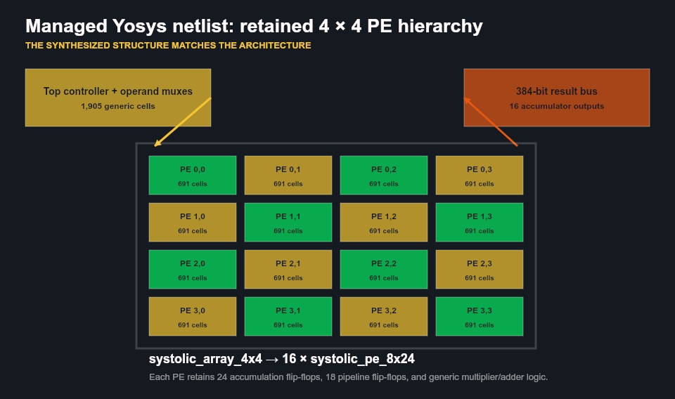
The managed netlist retained the array
The real netlist contains a top controller, result bus, and 16 hierarchical systolic_pe_8x24 instances rather than a flattened conceptual drawing.
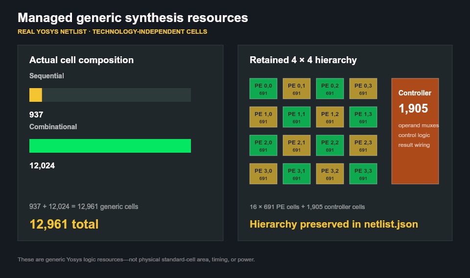
Actual synthesized logic composition
The chart is parsed from managed netlist.json: 12,961 technology-independent cells, split into 937 sequential and 12,024 combinational cells.
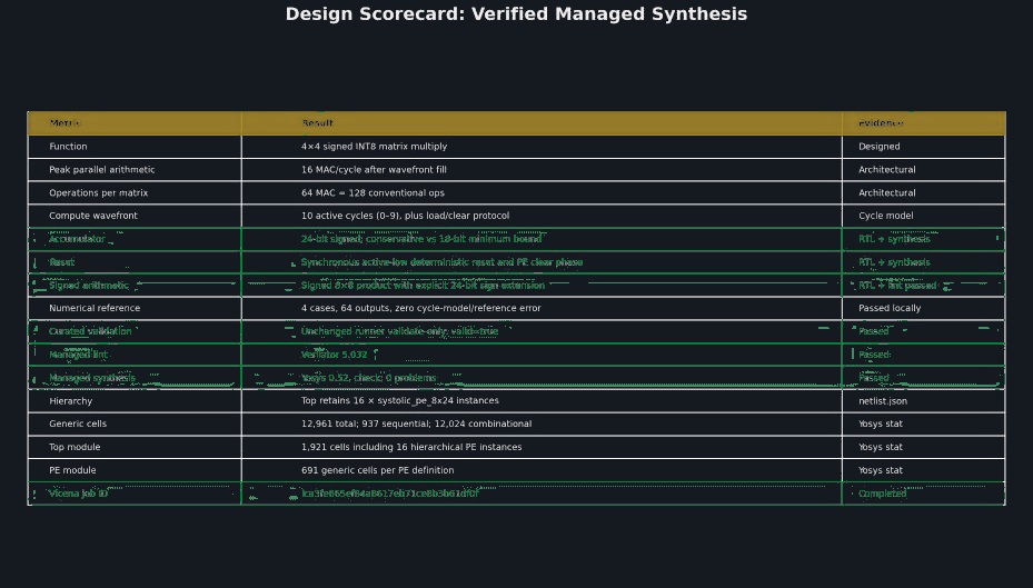
One scorecard connects intent to evidence
Architecture, arithmetic width, reset behavior, numerical reference, lint, synthesis, hierarchy, cell counts, job ID, and scientific boundaries stay together.
Connected R&D workflows
Research questions, process evidence, and design artifacts stay connected.
Semiconductor development spans more than RTL. Vicena can keep lithography, metrology, defects, materials, experiments, device physics, circuits, and chip implementation connected without overstating what any one workflow proves.
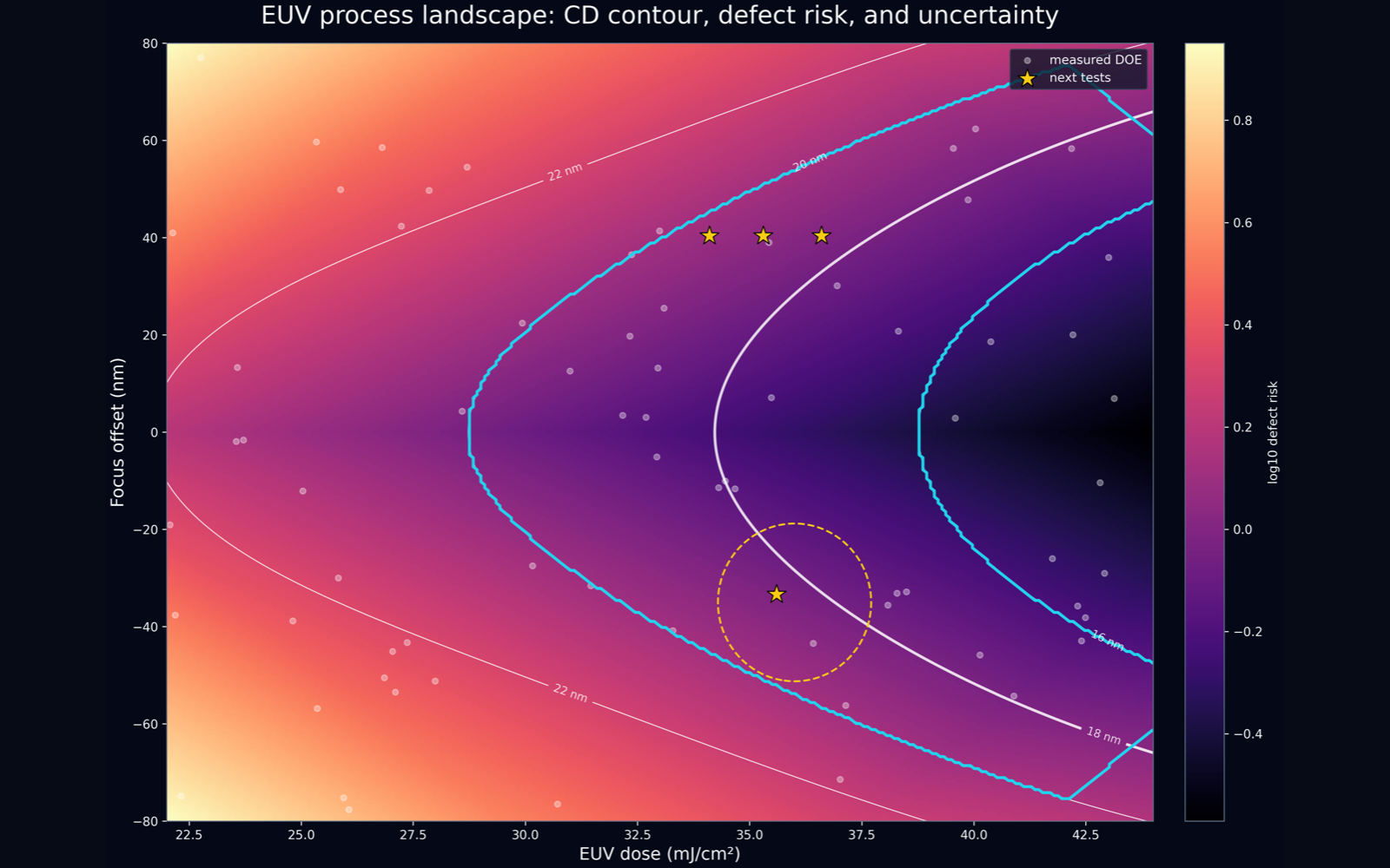
Lithography process development
Analyze focus-exposure matrices, Bossung curves, process windows, CD response, stochastic variability, and next DOE points.
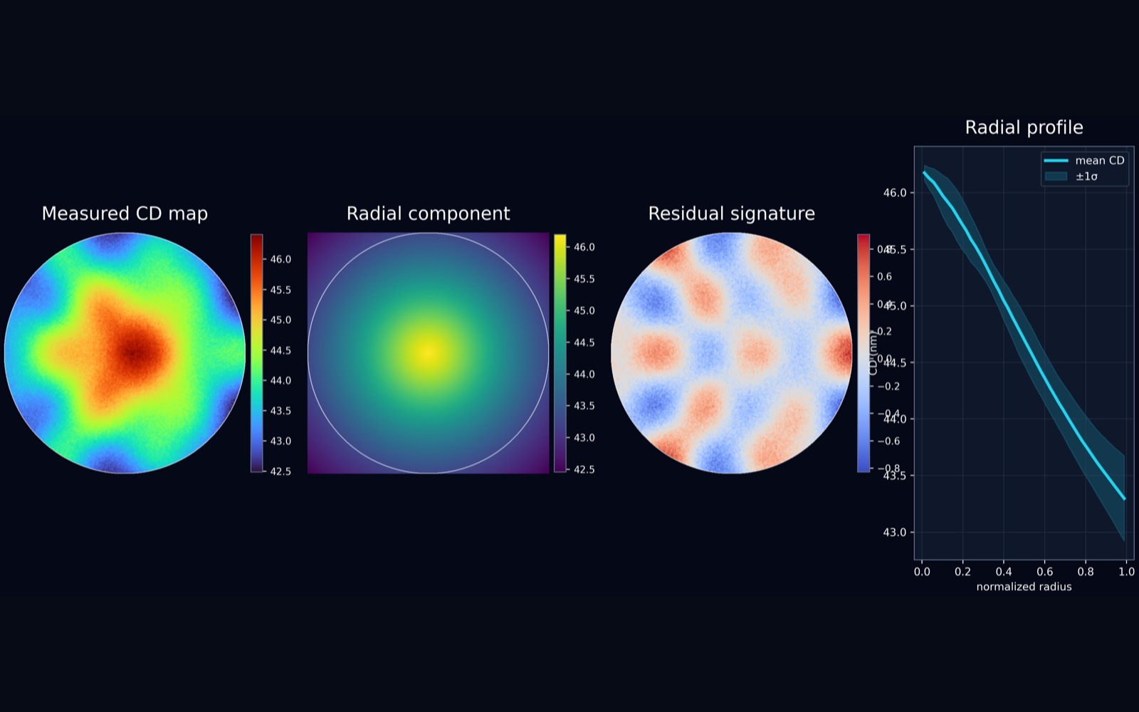
Wafer-map and metrology analytics
Decompose wafer-level signatures into radial trends, residuals, field effects, outliers, CDU, overlay, film thickness, and defect distributions.
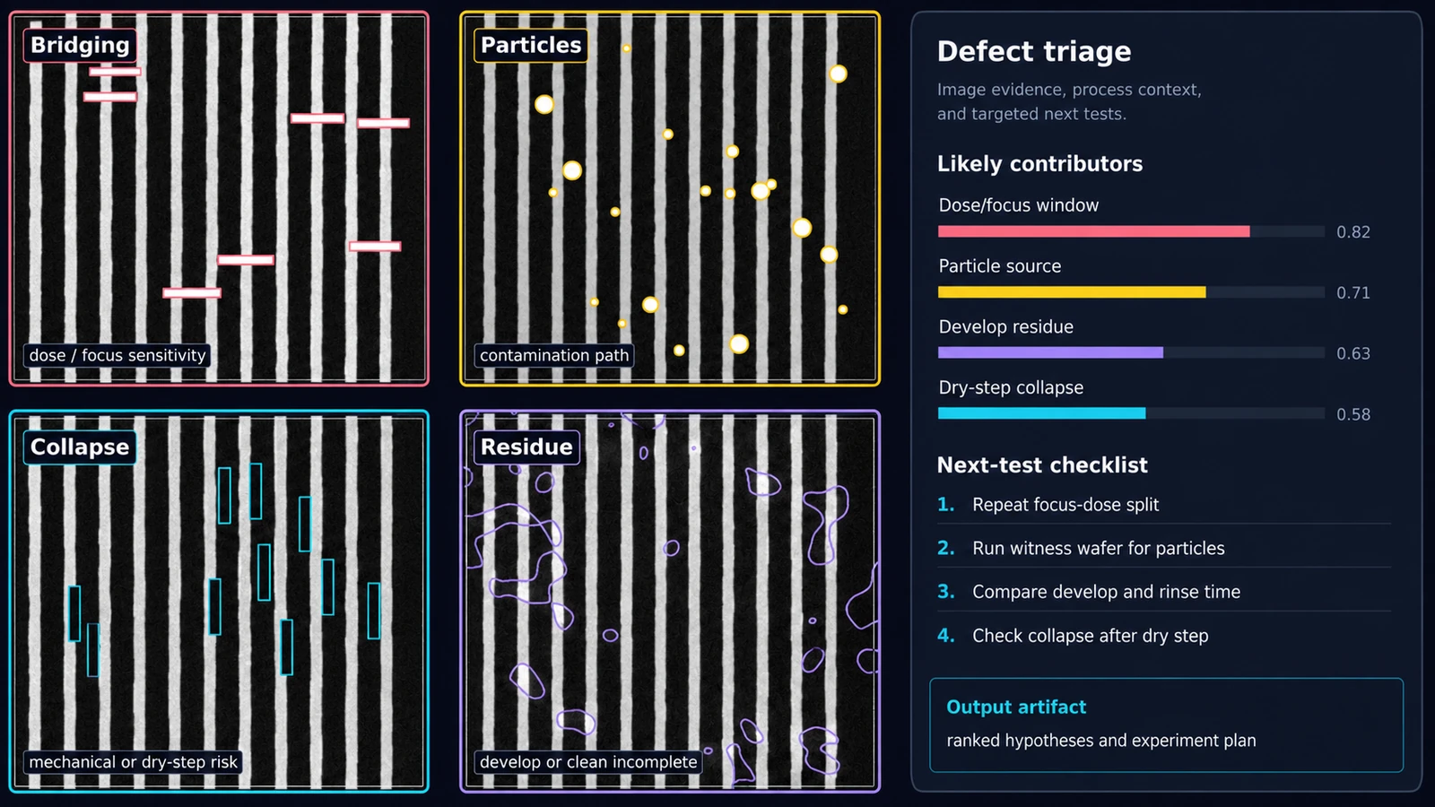
Defect and failure analysis
Cluster defect morphologies, connect process changes to failure hypotheses, and produce targeted next-test plans for review.
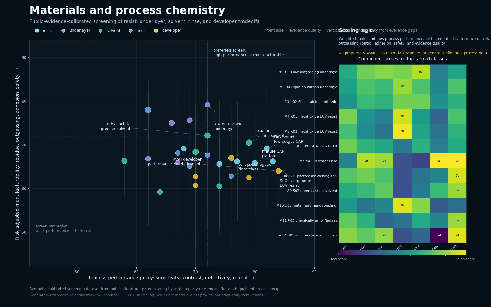
Materials and process chemistry
Screen candidates for compatibility, residue risk, outgassing concern, solubility, hazards, process performance, and supporting evidence.
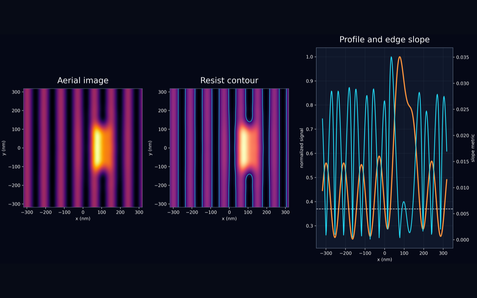
Aerial image and resist contour modeling
Explore how pattern geometry, source assumptions, threshold behavior, printed contours, and edge slope affect lithography decisions.
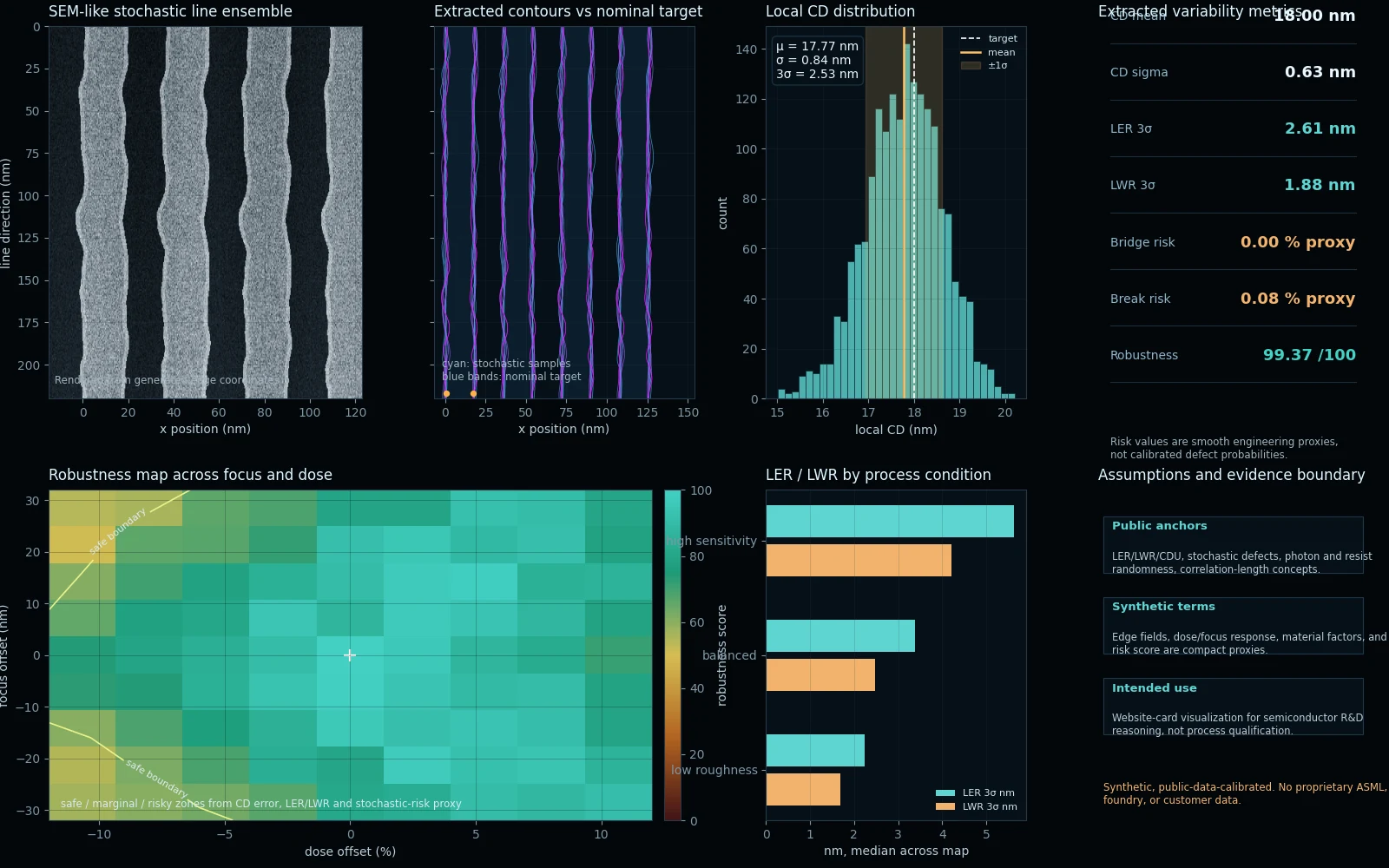
Stochastic variability and robustness
Visualize line-edge ensembles, CD distributions, process uncertainty, and robustness against focus, dose, and material variation.
Scientific packages
The scientific packages behind digital, physical, and device design.
-
Icarus Verilog
12
RTL simulation
Compiles Verilog and SystemVerilog testbenches, executes them with vvp, and produces inspectable VCD waveforms.
Official project -

Verilator
5.032
SystemVerilog lint
Finds syntax, width, signedness, unreachable logic, and other RTL problems before synthesis or implementation.
Official project -

Yosys
0.52
Logic synthesis
Transforms RTL into technology-independent netlists and reports hierarchy, cells, memories, and structural checks.
Official project -

OpenROAD
public 26Q3 workbench
RTL-to-GDS physical design
Carries suitable designs through floorplanning, placement, clock-tree synthesis, routing, timing, and public-PDK implementation.
Official project -

KLayout
Layout and GDS inspection
Generates and inspects GDS layouts and supports physical-verification work around public semiconductor platforms.
Official project -
DEVSIM
2.10
Semiconductor-device simulation
Solves drift-diffusion and related device equations for diodes, transistors, materials, contacts, and electrical characteristics.
Official project
Scientific capabilities
A path from algorithms toward open silicon.
Vicena can connect multiple open-source design layers while keeping their claims separate: mathematical reference, RTL behavior, logic synthesis, device physics, circuits, and physical implementation.
Evidence intake
Turn early technical questions into cited literature briefs, patent landscapes, material comparisons, and open-question lists.
Experiment planning
Convert evidence and hypotheses into DOE tables, metrology plans, controls, acceptance criteria, and next-test recommendations.
RTL architecture and verification
Develop Verilog designs, explicit interfaces, reset behavior, pipelines, test strategies, lint checks, and numerical references.
Notebook execution
Use reproducible notebooks for process windows, wafer maps, defect metrics, surrogate models, and data analysis that can be inspected later.
Decision artifacts
Generate technical briefs, CSV tables, figures, notebooks, compatibility memos, method drafts, and review-ready reports.
Open-source logic synthesis
Use managed Verilator and Yosys workflows to inspect warnings, hierarchy, netlists, generic cells, and synthesis checks.
Public-PDK implementation
Extend suitable designs toward OpenROAD-based floorplanning, placement, routing, timing, DRC/LVS, and reproducible RTL-to-GDS studies.
Device and power-electronics research
Connect DEVSIM device models, ngspice circuits, control electronics, and open semiconductor workflows without conflating their evidence levels.
Evidence discipline
The correction is part of the record.
Production-quality design is not the absence of warnings. It is the ability to stop on a real issue, change only what the evidence supports, and preserve the successful and failed artifacts needed to audit the decision.
Scientific boundary
Synthesized RTL is not a manufactured chip.
Start with your design
What should your next open chip do?
Describe the behavior and constraints. Vicena can structure the design, choose the appropriate open workflow, and keep every verification layer visible.