
Public service evidence
Microelectronics Research Center (MRC)
Microelectronics Research Center (MRC) at The University of Texas at Austin provides shared-facility access for nanofabrication and microfabrication, and surface and thin-film characterization. Registration, training, project review, fees, and current instrument availability may apply.
External services publicly offered
Publicly described capabilities
Fabrication
Nanofabrication and microfabrication
Advanced characterization
Surface and thin-film characterization
Explore the equipment
Instrument models
CAD illustrations show the instrument model. Confirm the installed configuration and current availability with the lab.
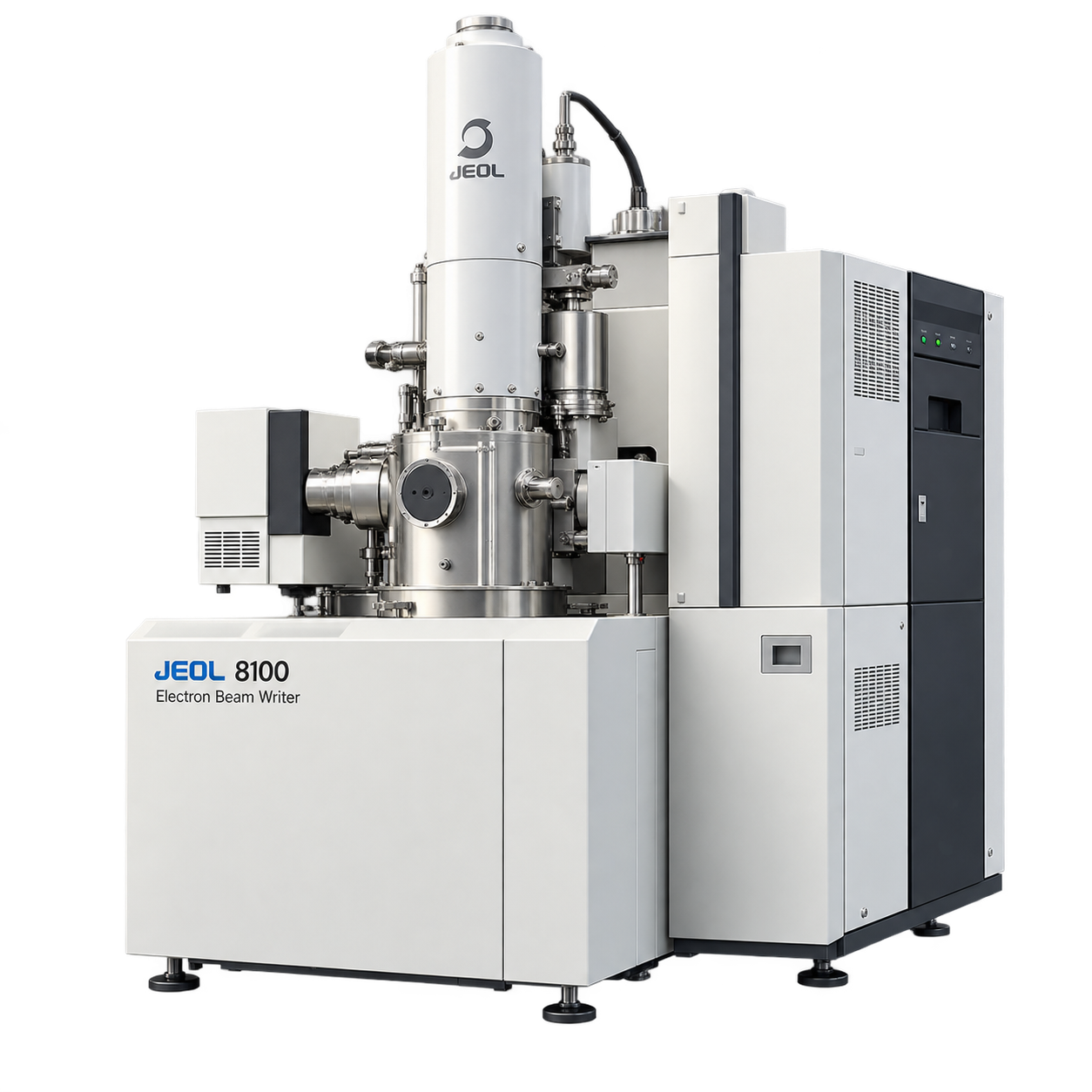 Model illustration
Lithography system
JEOL 8100
Equipment evidence
JEOL 8100 electron-beam writer in MER 1.720A.
Source 1 ↗Source 2 ↗Source 3 ↗Source 4 ↗Source 5 ↗Source 6 ↗Technical inventory
Techniques and equipment
-
Micro/nanofabrication
cleanroom process equipment
-
Micro/nanofabrication
electron-beam lithography system
-
Laboratory equipment
nanoscale metrology instrument
-
Micro/nanofabrication
plasma etching system
-
Laboratory equipment
semiconductor process equipment
-
Micro/nanofabrication
thin-film deposition system
-
Micro/nanofabrication
Cambridge NanoTech Savannah 200 atomic-layer-deposition system in MER 1.704.
-
Micro/nanofabrication
Corial210 chlorine ICP etcher for III-V materials and Corial210 fluorine ICP etcher for silicon, in MER 1.736 and 1.738 respectively.
-
Micro/nanofabrication
Fiji F200 atomic-layer-deposition system with remote plasma and ozone generator in MER 1.756.
-
Spectroscopy
J.A. Woollam IR-VASE, M-2000 DI and RC2 ellipsometers listed in the facility tool directory.
-
Laboratory equipment
JEOL 8100 electron-beam writer in MER 1.720A.
-
Micro/nanofabrication
Raith E-line electron-beam lithography system in MER 1.730A.
-
Microscopy & imaging
Two Bruker Icon atomic force microscopes in MER 1.728.
Registry scope evidence
- ◇Facility: 12,000 square feet of shared class 100/1000 cleanroom supports silicon, III-V and soft materials..
- ◇Capabilities: Sub-20 nm e-beam lithography, deposition, etching, thermal processing and characterization are offered..
- ◇Address: Official contact page identifies Building 160 at J.J. Pickle Research Campus..
- ◇Official-source, facility-specific instrument evidence is available. Current configuration, availability, price, and project fit require confirmation.
Evidence used for this listing
Vicena compiles these public listings from cited laboratory sources. A listing does not imply a partnership, current availability, pricing, or acceptance of a project. This profile is not an endorsement, availability check, quote, or representation of a commercial relationship.