
Public service evidence
Cornell NanoScale Science & Technology Facility (CNF)
Cornell NanoScale Science & Technology Facility (CNF) at Cornell University provides shared-facility access for nanofabrication and microfabrication, surface and thin-film characterization, and optical microscopy and spectroscopy. Registration, training, project review, fees, and current instrument availability may apply.
External services publicly offered
Publicly described capabilities
Fabrication
Nanofabrication and microfabrication
Advanced characterization
Surface and thin-film characterization
Advanced characterization
Optical microscopy and spectroscopy
Explore the equipment
Instrument models
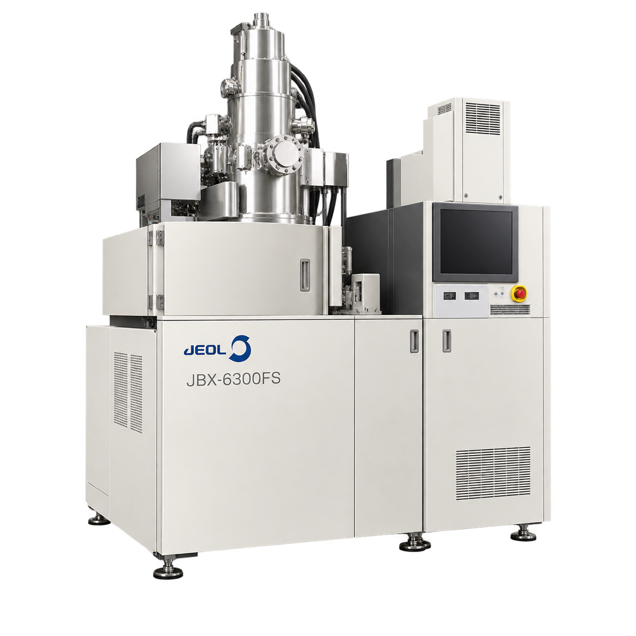
CAD illustrations show the instrument model. Confirm the installed configuration and current availability with the lab.
 Model illustration
Other laboratory / process equipment
JEOL JBX-6300FS
Equipment evidence
JEOL JBX-6300FS electron-beam lithography system
JEOL JBX-6300FS supports direct-write EBL on wafers to 150 mm with sub-10-nm capability.
Source 1 ↗Source 2 ↗Source 3 ↗Source 4 ↗Source 5 ↗Source 6 ↗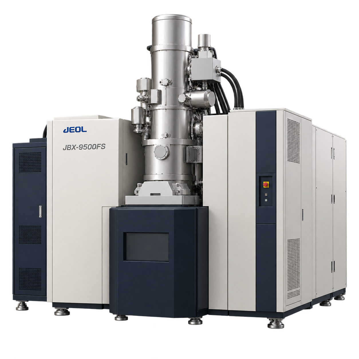 Model illustration
Other laboratory / process equipment
JEOL JBX-9500FS
Equipment evidence
JEOL JBX-9500FS electron-beam lithography system
JEOL JBX-9500FS EBL operates at 100 kV with 100 MHz clock and 1 x 1 mm write field, handling 10 mm pieces through 300 mm wafers and sub-10-nm features.
Source 1 ↗Source 2 ↗Source 3 ↗Source 4 ↗Source 5 ↗Source 6 ↗Technical inventory
Techniques and equipment
-
Microscopy & imaging
Bruker Dimension Icon atomic force microscope
-
Micro/nanofabrication
JEOL JBX-6300FS electron-beam lithography system
-
Micro/nanofabrication
JEOL JBX-9500FS electron-beam lithography system
-
Laboratory equipment
Malvern NS300 NanoSight
-
Laboratory equipment
Malvern Nano ZS Zetasizer
-
Laboratory equipment
Nanonex NX-2500 nanoimprint system
-
Laboratory equipment
Oxford FlexAL ALD system
-
Microscopy & imaging
Zeiss Gemini SEM
-
Microscopy & imaging
Zeiss Supra 55VP field-emission SEM
-
Microscopy & imaging
Zeiss Ultra 55 field-emission SEM
-
Micro/nanofabrication
Cee Apogee resist spinners handle pieces through 200 mm wafers at more than 6000 rpm and up to 30000 rpm/s acceleration.
-
Micro/nanofabrication
Disco DA810 grinder processes silicon, glass, sapphire, SiC and III-V workpieces to 8 inches; Disco dicing saw supports multiple substrate classes.
-
Laboratory equipment
Finetech Fineplacer pico ma die bonder aligns chips to 20 x 20 mm over substrates to 100 x 100 mm with 5 micrometre placement accuracy and force to 20 N.
-
Micro/nanofabrication
JEOL JBX-6300FS supports direct-write EBL on wafers to 150 mm with sub-10-nm capability.
-
Micro/nanofabrication
JEOL JBX-9500FS EBL operates at 100 kV with 100 MHz clock and 1 x 1 mm write field, handling 10 mm pieces through 300 mm wafers and sub-10-nm features.
-
Micro/nanofabrication
Oxford PlasmaPro 100 Cobra 300 ICP-RIE accepts 100, 150 and 200 mm wafers and provides 3 kW ICP source plus optical endpoint detection.
-
Micro/nanofabrication
SUSS Gamma robotic coat/develop cluster handles wafer cassettes to 200 mm and includes AltaSpray for non-planar substrates.
Registry scope evidence
- ◇Access: Open user facility serving academic and company projects.
- ◇Commercial terms: Usage charged per hour by tool; industrial users pay market-equivalent rates.
- ◇Remote access: Some simple projects may be executed remotely by staff or independent contractors.
- ◇Official-source, facility-specific instrument evidence is available. Current configuration, availability, price, and project fit require confirmation.
Evidence used for this listing
Vicena compiles these public listings from cited laboratory sources. A listing does not imply a partnership, current availability, pricing, or acceptance of a project. This profile is not an endorsement, availability check, quote, or representation of a commercial relationship.